

Samsung Starts Construction of Advanced Chip Packaging Hub in South Korea
South Korea has begun building Samsung’s advanced semiconductor packaging facility in Chungcheong, marking a key step in its industrial development programme.

South Korea commenced construction of Samsung Electronics’ advanced chip packaging facility in Chungcheong, marking the first project under the government’s industrial megaproject and signalling a shift towards higher-value semiconductor manufacturing.
Quick Skim
Construction Begins on Chungcheong Advanced Packaging Hub
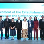
The groundbreaking ceremony took place in Asan, Chungcheong, with South Korean President Lee Jae-myung and Samsung Chairman Lee Jae-yong in attendance. The project intends to convert a decades-old semiconductor assembly and testing site into a centre specialised in high-bandwidth memory (HBM) packaging.
Samsung plans to invest 6 trillion won initially in establishing the advanced packaging facility at the Onyang campus, with further phased investments amounting to 40 trillion won aimed at procuring sophisticated equipment.
Part of Broader Industrial Development Programme
The facility is the first of three major industrial projects launched by the South Korean government in June, targeting growth areas such as semiconductors, artificial intelligence data centres, and physical AI. These initiatives also seek to stimulate investment outside the Seoul metropolitan region.
Leading semiconductor firms including Samsung Electronics and SK Hynix have announced combined investments totalling approximately 392 trillion won (US$295 billion) in Chungcheong over the longer term.
President Lee noted the rapid progress: “Just four months later, we are standing at the site where that promise is becoming reality.” Samsung’s chairman highlighted the site’s transformation over four decades from a basic assembly and testing plant into a centre for AI semiconductor innovation.
Implications for Semiconductor Supply Chains and Production
The development of an advanced HBM packaging hub will enhance South Korea’s semiconductor supply chain capabilities, supporting higher performance memory production essential for AI and high-performance computing applications. This investment is expected to optimise local manufacturing efficiency and help maintain the country’s competitiveness in global semiconductor markets.
Going forward, focus will remain on the phased deployment of equipment and expanding the facility’s capabilities, with progress closely watched as a signal of South Korea’s commitment to semiconductor industry leadership and regional industrial diversification.